Tuesday 20 December 2016

Why we need behavioral model+DB cell in Power aware simulation ?

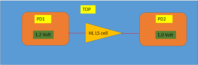
  •        Behavioural model is must for simulation tool.

o   Behavioural model is necessary for simulation tool to do functional checks . From DB it cannot retrieve functionality of that DB cell.
o   DB cell is required mainly to get PG pin related information as in non-power aware behavioural model you will not have PG pin information.
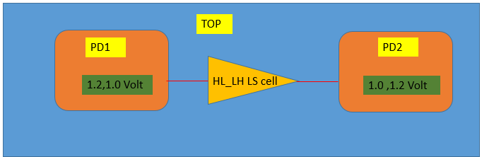
  •       DB information is optional .

o   If corresponding DB cell info is not provided than DB related checks will not be performed on that module and will be treated as simple Verilog module.
  •        Below points can be considered as general guideline.

o   If user have non-power aware behavioural model for DB cell , provide both DB info + behavioural model to simulation tool.

o   If user have Power aware behavioural model for DB cell , Only behavioural model is enough ,provided you do not want to do any DB related checks on it.

Sunday 18 December 2016

Do we need Power State Table (PST) for simulation tool ?

Yes it is needed for Low Power coverage analysis . Simulation tool does coverage analysis based on PST written by user.

Monday 12 December 2016

Default value of power and ground net

By default state and voltage value for power and ground net should be as follow.


Wednesday 23 November 2016

Strategy will be applied on which ports if no filter is used in strategy?

In below case which are the target ports for isolation ?


module top ();
core1 CORE1 (.*);
endmodule

module core1 (input in1, in2 ,outpot out1);
assign out1 = in1 & in2 ;
endmodule


create_power_domain PD1 -elements {CORE1}
set_isolation iso_1 -domain PD1


>> Here as no filter is specified by default all the i/p and o/p ports of CORE1 are target port for strategy  "iso_1" .


Precedence rules in UPF Strategy

User can specify different strategy which may refer to same element , but with different options in strategy.
Let us take example of isolation strategy .

If user has below UPF isolation strategies which one is takes the higher precedence .

set_isolation iso_1 -domain PD1

set_isolation iso_2 -domain PD1 -applies_to outputs

set_isolation iso_3 -domain PD1  -source PD1.primary

set_isolation iso_4 -domain PD1 -sink TOP.primary

set_isolation iso_5 -domain PD1 -source PD1.primary -sink TOP.primary

set_isolation iso_6 -domain PD1 -elements {CORE1}

set_isolation iso_7 -domain PD1 -elements {CORE1/out1}

set_isolation iso_8 -domain PD1 -elements {CORE1/out1[1]}


>> Here highest precedence will be given to strategy "iso_8" . Similarly 2nd priority to "iso_7" and so on.


Friday 7 October 2016

How connect_supply_net command used to override default PG pin connection of any cell

By default any logic/cell in the given by power domain will use the domain primary supply to power that logic. To override this default rule user can explicitly write connect_supply_net command to connect the any specific PG pin of the cell with needed supply net in UPF.

Let us understand this with example.
Why this is needed . Consider a level shifter cell , which has 2 power net. Now connecting both the power net to a domain primary power net will end up in electrical problem. So one PG pin can be connected to domain primary power net which will be by default. For another PG pin we can use connect_supply_net command to connect it to a required supply net in UPF.


Design :


module top (in1,..);

LS_CELL i_ls (.A(in1),.Z(w1));

endmodule

UPF:

create_supply_net VDD
connect_supply_net VDD -ports {i_ls/VDD1}

What is Power Domain in UPF?

Power Domain is common term used in UPF language. Power Domain is abstract way to include the instances/block . Instances/block that shares the same supply should be included in one power domain.  At the end all design instances should be part of any Power domain . Also one instance can not be part of more than one power Domain. If user has not included any instance in any Power Domain using create_power_domain command then it will be a part of it's ancestor's Power Domain.

Defining Power Domain is necessary to implement all Low Power checks.

Let us consider below example .

In My Soc I have three block.i.e Block1 , Block2, Block3 .

Now in order to do low power checks on this Soc , Based on the architectural level details i.e which block can work on what voltage and when any block can be shutoff , User needs to create power domains as a starting point in UPF.

Let us say as per spec Block1 and Block2 will always operate on same voltage then I can place them in 1 power Domain .And As Block 3 can operate on different voltage and can be shutoff independently I will put in other domain.

And TOP block where all of this block will be instantiated will be placed in 1 domain.

This can be coded in UPF as below.

UPF code:

create_power_domain TOP -elements {.}
create_power_domain PD1 -elements {Block1 Block2}
create_power_domain PD2 -elements {Block3}


This way you can partition your design instances in separate power domain based on the power specification .

Tuesday 27 September 2016

Does the state defined on Supply Set propagates to associated supply nets?

We defined a state on supply set through add_power_state command in UPF. Also the supply is having different function i.e power,ground,nwell,pwell . Let us understand this by example.


create_supply_set SS -function {power VDD} -function {ground VSS}
add_power_state SS -state {ON  –simstate NORMAL -supply_expr {(power == {FULL_ON 0.8})}

create_pst pst_1 -supplies {VDD}
add_pst_state  s1 -pst pst_1 -state {ON}


Typically many user write their UPF in above way . State "ON" is defined on Supply Set "SS" . But user uses this state name for "VDD" in PST table which associated with Supply Set "SS".

This is wrong usage as per UPF LRM. 

State which is defined on Supply Set is limited to Supply set only and not supposed to be propagated to associated supply net.

Now the question is why state should not be allowed to propagates on supply nets.

consider a below case.

create_supply_set ss_top
create_supply_set ss_pd1 -function {power ss_top.power}

add_power_state ss_top -state {ON  –simstate NORMAL -supply_expr {(power == {FULL_ON 0.8})}
add_power_state ss_pd1 -state {ON  –simstate NORMAL -supply_expr {(power == {FULL_ON 1.0})}

Here  ss_pd1.power is connected to ss_top.power.

If we allow propagating supply set state to supply nets . We have below issue .

With add_power_state used above user is trying to create state named "ON" with value 0.8 and 1.0 on same net. This is not possible as same net can not have different voltage value with same state name.

So this issue will get resolved if we do not propagates the state names to associated supply nets.

Tuesday 20 September 2016

What is lower domain boundary concept in UPF?

Idea of lower domain boundary is introduced to allow adding isolation at top level for macro/ip in which directly you can not add isolation during SOC level integration.


Consider a below case to understand this .


Here for the TOP level domain only TOP o/p port is considered as power domain boundary port if lower domain boundary concept is not there. But with lower domain boundary support o/p port of PD1 is also visible in TOP domain and it is known as lower domain boundary port for TOP domain.


Here PD1 o/p is connected to TOP o/p port. Now in order to place isolation cell b/w PD1 o/p port and TOP o/p port , In usual way we write below strategy.

set_isolation  iso_1 -domain PD1 -elements {CORE1/out} -location parent

But if you do not have have the access of UPF file of PD1 domain , considering it is so,me third party IP. So in that case the who integrates this IP in top level has to write isolation strategy as below.


set_isolation  iso_1 -domain TOP -elements {CORE1/out} -location self

Tuesday 13 September 2016

What is location fanout in UPF ?

Certain UPF command has -location switch . i.e set_isolation , set_level_shifter . Again -location can be "fanout".

Consider a below example to understand that how isolation cell will be inserted/placed by synthesis tool when -location fanout is specified .

Here domain PD1 domain o/p signal is going to two different domain PD2 and PD3 .So this is a case of fanout .

Now if user has isolation strategy on PD1 domain with -location fanout , Isolation cell will be inserted as shown in figure under Netlist option (named as ISO) .


UPF:

set_isolation iso_1 -domain PD1 -applies_to outputs -location fanout


RTL:


Netlist:


What is the use of set_retention_elements command from user prospective?

UPF has command set_retention_elements . This command is used to create list of signals/register which are supposed to be retained . This list will be used in set_retention -elements command.

Now the question is if we are directly able to specify the signal/register name in set_retention -elements command , why we need to create the list using set_retention_elements command and then using it in set_retention -elements .

Answer to this question is that when any third party vendor is creating an IP for any block and developing UPF for the same . At that time he does not have the information that if this block will be shutdown when used in SOC level by end user. So what he will do is just give the list of signal/register which are important and need to be retained by the user if domain in which this block will be placed is shutdown . So this list he will provide using set_retention_elements command .

Now if end user need this block to be in switchable domain , he need to write retention strategy for the elements specified in the list created by set_retention_elements . This way end user need not to analyse the internal of the IP block. And will serve the purpose of retaining important registers as well.

Also if the end user does not know the critical registers he has to retain all registers in the IP. Which can lead to area overhead and which might not be be required as all the registers might not be critical to be retained.


Example:

RTL:

module dut (input d,clk,rst, output reg q,q1) ;

always @ (posedge clk) begin
  if (!rst)
       q <= 0;
 else
      q <= d;
end

always @ (posedge clk) begin
  if (!rst)
       q1 <= 0;
 else
      q1 <= d;
end
endmodule

UPF:

set_retention_elements ret_list -elements { q q1}
set_retention ret_1 -domain TOP -elements {ret_list}


Monday 12 September 2016

What is the use of logic port/net created using UPF command ?

UPF LRM has below commands for creating logic port/net and connect them . Question comes to user that what is the use of creating logic(design) port/net through UPF command.

cretae_logic_port
create_logic_net
connect_logic_net

Generally this is mainly used for creating control port/net used in the other UPF commands.

Let us take one example for isolation.

At RTL level let's say user is writing a isolation strategy in his UPF. Now user does not have the isolation control signal defined in the design . So in alternative way he can define isolation control signal using cretae_logic_net command and then use it as isolation signal in isolation strategy. So at the time of Netlist creation , Synthesis tool will create a port/net in actual design with the same name.
This way user can avoid defining UPF control signals in design at RTL level.

RTL:

module dut (in1,in2,out);
input in1,in2;
output out;

assign out = in1 & in2;

endmodule

UPF:

create_power_domain TOP
create_logic_port iso_en
create_logic_net iso_en
connect_logic_net iso_en -ports iso_en

set_isolation iso_1 -domain TOP  -clamp_value 0
set_isolation_control iso_1 -domain TOP -isolation_signal {iso_en} -isolation_sense low -location self

Netlist :

module dut (in1,in2,out,iso_en);
input in1,in2;
input iso_en;
output out;

AND (in1,in2,w1);
ISO (w1,iso_en,out1) ;

endmodule

Sunday 21 August 2016

Types of power consumption

There are basically two types of power consumption.

1. Dynamic

  • Dynamic power is consumed during switching of transistors , And hence it depends on clock frequency and switching activity.  
  • Dynamic power has two components. 
    • Switching power
      • This is the power that requires to charge and discharge capacitive load during logic transition from 1 to 0 and vice-versa.
    • Internal power
      • This is the power that consumed during transition . i.e. A point where both NMOS and PMOS are ON . Which is called as crowbar current.


2. Static

  • Static power is transistor leakage current that flows when we apply power to a device.
  • Main causes of static power consumption are as below.
    • Reverse bias p-n junction leakage diode.
    • sub-threshold leakage.
    • Gate leakage.

Different power consumption reduction techniques

Different types of strategies used to reduce power consumption. Some of them are listed as below.

1. Clock gating

  • It is a technique through which clock signal is changed to a value such that there is no requirement of evaluating registers whose value is not supposed to be changed for specific time interval. This will ensure that there is no switching activity due to change in clock and hence reduction in dynamic power consumption.

2. Power gating

  • Power gating is a technique to shut down the power of a block when it is not required to be On. i.e In Mobile voice processing block can be shutdown when user is not having incoming or outgoing call . This is the best method of reducing power consumption. 

3. Multiple Vt Library cells

  • Nowadays user provides same cells with two different threshold voltage in library. So that synthesis tool can choose cell depending on requirement. With low Vt , sub-threshold leakage will increase but speed will also be higher. So for timing critical path synthesis tool will insert low Vt cells and at other path high Vt cell .

4. Dynamic voltage and frequency scaling

  • In this technique same block can be working at different voltage at different time .i.e some time it is required to do high computation (complex equation solver) task then it needs more speed so it can operate at high voltage . While some time low computation is required so it can operate at lower voltage.

5. Supply voltage reduction

  • As power is directly proportional to voltage (p =iv ) , with reduction in voltage ,power consumption will reduce. But again with reduction in voltage will reduce switching speed as well. 

6. Multi voltage design

  • In SOC some block ( RAM) are such which requires higher speed , so that block can be powered with higher voltage . While some block (Peripheral device) which does not needs high speed so that block can be powered with lower voltage , which in turn can reduce leakage power . In earlier days people used to have same voltage for whole design which makes it necessary to operate it high voltage . While this new technique we can achieve leakage reduction.

Tuesday 26 July 2016

Why Isolation is required b/w ON to OFF(Standby) block ?

Generally we see that Isolation is required b/ OFF to ON block. But in some design isolation cells are inserted b/w ON to OFF(More correct to say standby) block as well. This is called as Parking .

This is required for some signals which are having many load in OFF(Standby) block. i.e clock/reset. This will insure that clock/reset does not toggle when domain is in OFF(Standby) state. And which in turn will prevent switching/toggling of many sequential elements in shutdown domain . And hence we can reduce power consumption.

Low Power Sequence

In general below sequence is followed in Low Power related design.

1. Save the register/flop o/p.
2. Enable isolation.
3. Clock gating.
4. Shutdown power domain.
5. Wait for specific time period.
6. Switch On power domain.
7. Restore the saved value on register/flop.
8. Clock un-gate.
9. Disable isolation.


Monday 25 July 2016

How clock gating is used to reduce Dynamic Power consumption?

Clock gating is the effective way to reduce Dynamic/Switching power consumption. When the user knows my domain is in standby state , user can easily gate(block) the clock used in Flip-flops (sequential elements) in that power domain . So when there is no activity on clock , Sequential elements will not have to change their states . Which in turn will reduce the Power consumption as more the switching more power consumption.

Generally clock gating is done by adding extra clock gating logic in the path of original clock . i.e original clock is "clk" and control pin to gate this clock this "clk_cntrl" . So an AND gate logic is inserted which has to i/p "clk" and "clk_cntrl" . And o/p is "clk_gated" , which will will be then used in all sequential logic as final clock.


Verilog code:

assign clk_gate = clk & clk_cntrl ;

always @ (posedge clk_gate) begin
  if (!rst) q <= 0;
 else q <= d;
end


>> This way when domain is going in standby mode, value of "clk_cntrl" can be changed to logic 0. So that signal "clk_gate" will also  become 0 and hence there will not be any switching activity on flop .


>> User can verify that clock gating is done properly or not using writing some custom assertion.

i.e Consider a example where "standby_ctrl" is control pin used to put domain in standby(COA) mode . when "standby_ctrl" is 1 , domain is in standby mode.


So below piece of code can be written in testbench to verify clock gating logic.

always @(standby_ctrl) begin
  if (psw_ctrl)  begin
     assert (clk_gate == 0 );
    else $error ($time,"CLK_GATING not active when domain is in standby(COA) state");
 end
 else begin
   assert (clk_gate == clk );
    else $error ($time,"CLK_GATING  active when domain is in ON state");
 end
end

Tuesday 12 July 2016

Power Switch cells and strategy in Power aware design and UPF


Overview:
  • Power Switch cells are used for Power distribution in Power aware design. 
  • These are typically inserted by Placement and routing tool (i.e ICC).
  • To let tool insert a PSW cells in the design , At RTL stage user needs to define Power switch strategy in UPF using create_power_switch command.

Types of Power switch cells:

Depending on liberty attribute:

1. Fine grain :
  • Liberty attribute : switch_cell_type : fine_grain;

2. Coarse grain :
  • Liberty attribute : switch_cell_type : coarse_grain;


Depending on Power/Ground Routing:

1. Header switch :
  • This is for routing Power Net. PMOS is used for constructing this type of PSW cells as PMOS is good to pass logic 1 .

2. Footer switch :
  • This is for routing Ground Net. NMOS is used for constructing this type of PSW cells as NMOS is good to pass logic 1 .

Example: 

UPF:

create_power_switch sw_1 -domain TOP
-output_supply_port {psw_out VDD_PSW}
-input_supply_port {psw_in VDD}
-control_port {ctrl_psw sw_en}
-on_state {PSW_on vin { ctrl_psw }}
-off_state {PSW_off { ! ctrl_psw}}


Wednesday 29 June 2016

What is Level-Shifter cells ?


Two interacting power domains may also be operating with different voltage ranges. In this case, a logic 1 value might be represented in the driving domain using a voltage that would not be seen as an unambiguous 1 in the receiving domain. i.e receiving domain might treat it as 0 due to high operating voltage .

Level-Shifters are inserted at a domain boundary to translate from a lower to a higher voltage range, and sometimes from a higher to a lower voltage range as well. The translation ensures the logic value sent by the driving logic in one domain is correctly received by the receiving logic in the other domain.

Level-Shifter cells are functionally similar to Buffer cell.


Types of Level-Shifter Cells :

1. HL : High to Low type of LS cell is required when source domain is operating at high voltage and sink domain is working at low voltage in any specific state of PST(Power-State Table).


2. LH : Low to High  type of LS cell is required when source domain is operating at low voltage and sink domain is working at high voltage in any specific state of PST(Power-State Table).


3. HL_LH : This is the type of LS cell which will serve both purpose i.e it can convert signal voltage to low to high and vice versa. This type of cell is mainly required when in 1 PST state source domain is operating at high voltage and sink domain is working at low voltage while in another PST state source domain is operating at low voltage and sink domain is working at high voltage.


Liberty attributes of LS cell :

  • is_level_shifter : true;  
    • This attribute says that it is LS type cell.
  • level_shifter_type : LH; 
    • This attribute says it is LS cell of of type LH.

What is ELS (Enable-Level Shifter) cell ?

Enable-Level Shifter cells often termed as ELS cells. This are cells which has the functionality of both Isolation and Level-shifter cells. In general this will serve the purpose of both isolation and level-shifting in Power-Aware designs .

This will have the advantage that it will occupy less area compared to separate isolation and level-shifter cell.

Why State retention (Retention) is required in Power-Aware Design ?


  • State retention is the ability to retain the value of a state element in a power domain while switching off the primary power to that element, and being able to use the retained value as the functional value of the state element upon power-up. 

  • State retention can enable a power domain to return to operational mode more quickly after a power-down/power-up sequence and it can be used to maintain state values that cannot be easily recomputed on power-up. State retention can be implemented using retention memories or retention registers. Retention registers are sequential elements (latches or flip-flops) that have state retention capability.

What is Isolation cells in Power aware Design?


Why Isolation cell is required in Power Aware Design?
  • Two power domains interact if one contains logic that is the driver of a net and the other contains logic that is a receiver of the same net. When both power domains are powered up, the receiving logic should always see the driving logic’s output as an unambiguous 1 or 0 value, except for a very short time when the value is in transition. The structure of CMOS logic typically ensures that minimal current flow will occur when the input value to a gate is a 1 or 0. However, if the driving logic is powered down, the input to the receiving logic may float between 1 or 0. This can cause significant current to flow through the receiving logic, which can damage the circuit. An undriven input can also cause functional problems if it floats to an unintended logic value.
  • To avoid this problem, isolation cells are inserted at the boundary of a power domain to ensure that receiving logic always sees an unambiguous 1 or 0 value. Isolation may be inserted for an input or for an output of the power domain. An isolation cell operates in two modes: normal mode, in which it acts like a buffer, and isolation mode, in which it clamps its output to a defined value. An isolation enable signal determines the operational mode of an isolation cell at any given time.

Types Of Isolation Cells :

Depending upon the need of user , There are mainly three types of isolation cells.

1. Isolation cell with clamp_value 1:
  • This type of Isolation cells will have function such that it will have o/p of logic 1 , when it is in isolation mode. And when it is in non-isolation mode it will act as buffer i.e simply pass the data to o/p. This is similar to OR gate.
2. Isolation cell with clamp_value 0:
  • This type of Isolation cells will have function such that it will have o/p of logic 0 , when it is in isolation mode. And when it is in non-isolation mode it will act as buffer i.e simply pass the data to o/p.This is similar to AND gate.
3. Latch type Isolation cell:
  • This type of Isolation cells will have function such that it will latch the o/p of isolated port when it is in isolation mode. And when it is in non-isolation mode it will act as buffer i.e simply pass the data to o/p.This is similar to Latch.

Types of Retention Cells

Depending on how the retained value is stored and retrieved/restored , there are at least two flavors of retention registers, as follows:

1) Balloon-style retention: In a balloon-style retention register, the retained value is held in an
additional latch, often called the balloon latch. In this case, the balloon element is not in the
functional data-path of the register. 

2) Master/slave-alive retention: In a master/slave-alive retention register, the retained value is held in the master or slave latch. In this case, the retention element is in the functional data-path of the
register.

  • Ballon-style retention can be Dual-Pin Retention cell or Single-Pin Retention cell. 
  • Master/slave-alive retention is same as Zero-Pin Retention cell.

Dual-Pin Retention :
  • Dual-Pin Retention is the one which has two separate control signal for save and restore operation. 
  • Save operation can be level-sensitive or edge-sensitive.

Single-Pin Retention:
  • Single-Pin Retention is the one which has single control signal for both save and restore operation. 
  • Save operation can be level-sensitive or edge-sensitive.
  • Save operation and Restore operation will be on opposite level/edge of control signal. i.e If save is performed on level high than restore will be performed on level low of control signal.

Zero-Pin Retention:
  • Zero-Pin Retention is the one which does not have any control signal .
  • Save operation will be performed when the power domain in which cell is sitting goes from NORMAL to CORRUPT state. 
  • Restore operation will be performed when the power domain in which cell is sitting goes from CORRUPT to NORMAL state. 

Saturday 14 May 2016

Why UPF ?

UPF is language invented to allow user to do Low Power checks parallel to design flow. With UPF user can do Low Power checks at all stages of VLSI flow. i.e From RTL ,Netlist, PG-Netlist. UPF is written at RTL stage . User needs to define the power intent of his/her Design in the UPF file. Then user will take his RTL design and UPF to Synthesis tools like DC . Synthesis tool will add Low Power cells to Netlist Design based on what user has written in his/her UPF.